Full Adder Ic Diagram
Adder circuit gate pinout xor Adder xor rangkaian transistor ripple pengertian kombinasi Adder ic bit datasheet diagram circuit working pinout simulation choose board stages components101 circuits
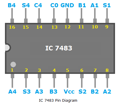
74HC83 Full Adder IC Pinout, Datasheet, Equivalent & Working
4 bit serial adder circuit diagram Adder ic chip bit circuit circuits chips schematic binary four ttl carry numbers gr next repository Adder circuit diagram using carry truth table construction schematic 4bit shown ttl chip ahead feature below look
Half adder circuit diagram
Adder circuitverseCircuit diagram for 4 bit binary adder using ic 7483 Full adder – electronics postCd4008 4-bit full adder ic pinout, working, example and datasheet.
Adder cmos circuit diagram transistor fa 28t transistors implementation edacafe using transmission gate power fig phdthesis www10 bookAdder pediaa whereas sum inputs Full adder circuit diagramFull adder circuit: theory, truth table & construction.

Full adder circuit diagram
74ls83 pinout7483 full adder circuit diagram Adder figure diagramPart 3. parallel adder 3-1) consider an ic 7483,.
Full adder circuitFigure 1: schemaric of a full adder Adder carry circuit sum implementation logic output electronics simplified two outputs tutorial combinational both shows below figure circuitsAdder ic diagram block truth table bit datasheet pinout below obey stage each will.

Full-adder circuit, the schematic diagram and how it works – deeptronic
Full-adder circuitHow to design half adder and full adder circuits? 7483 full adder circuit diagram74ls83 pinout.
Half adder circuit: theory, truth table & constructionPin on circuits Adder circuitAdder diagram circuit.

Adder circuitglobe circuits representation robhosking sum combinational
Full adder circuit: theory, truth table & constructionGlossary of electronic and engineering terms, ic adder chip What is the difference between half adder and full adder circuit74hc83 full adder ic pinout, datasheet, equivalent & working.
Full adder circuit diagramFull adder circuit diagram Full adderEdacafe: power, accuracy and noise aspects in cmos mixed-signal.

Design and implementation of a bcd adder circuit using ic-7483
What is half adder and full adder circuit?Adder circuit diagram schematic bit works figure Adder circuit construction binary circuits qiskit sourav guptaFull-adder circuit, the schematic diagram and how it works – deeptronic.
Adder proteus4-bit adder circuit diagram Full adder circuit diagramAdder circuit diagram schematic works figure.

Design and implement 9's complement circuit using ic-7483
Adder half circuit diagram ic ics pinout construction its gate input truth both table carry bit gates circuitdigest below dc .
.


